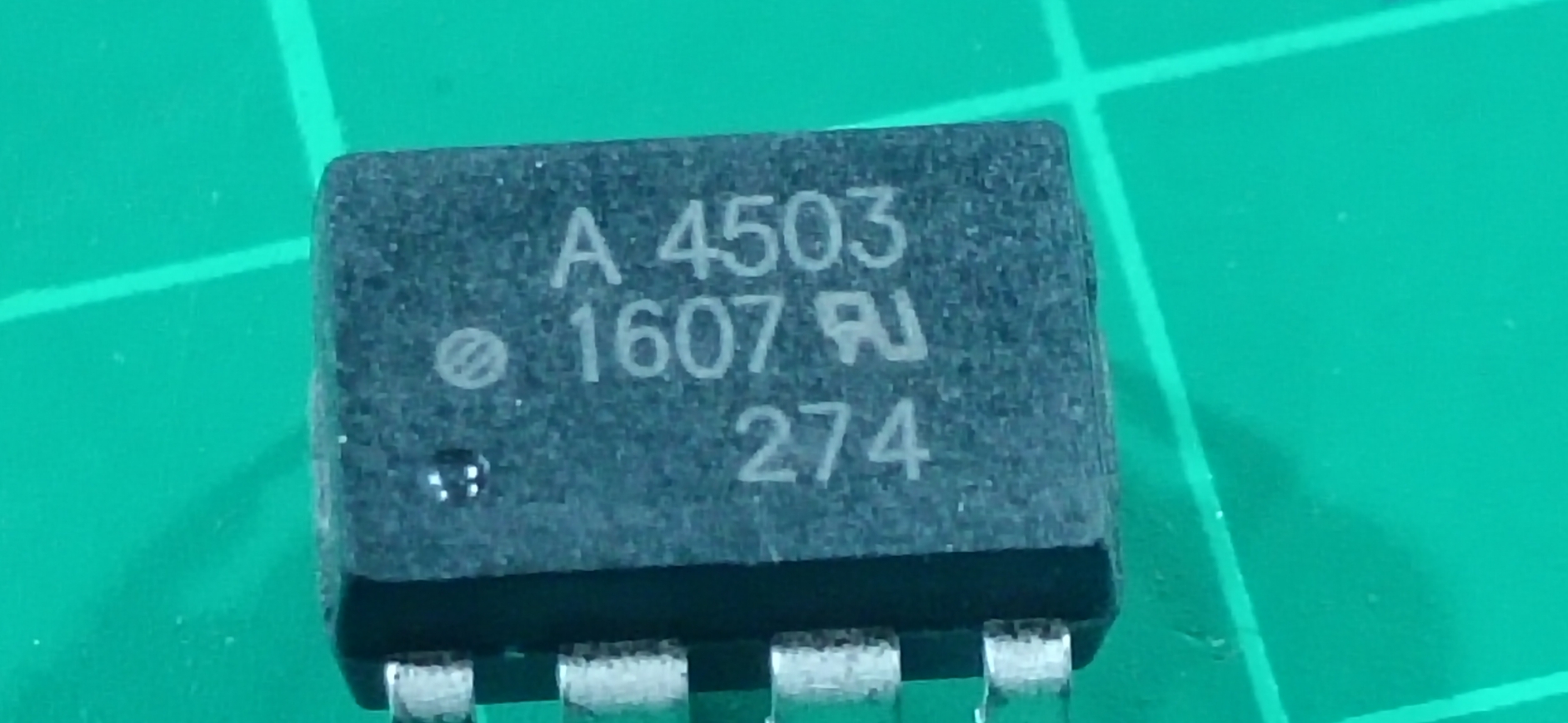
HCPL-4503 A4503 HP4503 IC OPTO ISOLATE

| รหัสสินค้า | SKU-00796 |
| หมวดหมู่ | ELECTRONIC PART FOR CNC REPAIR |
| ราคาปกติ | |
| ลดเหลือ | 65.00 บาท |
| ยี่ห้อ | AVAGO |
| รุ่น | HCPL-4503 A4503 HP4503 IC OPTO ISOLATE |
| สถานะสินค้า | พร้อมส่ง |
| สภาพ | สินค้าใหม่ |
| ลงสินค้า | 15 ม.ค. 2564 |
| อัพเดทล่าสุด | 20 พ.ค. 2568 |
| จำนวน | ชิ้น |
หยิบลงตะกร้า

รายละเอียดสินค้า
HCPL-4503 A4503 HP4503 IC OPTO ISOLATE
DATA SHEET https://pdf1.alldatasheet.com/datasheet-pdf/view/112437/HP/HCPL-4503.html
Small Outline, 5 Lead, High
Speed Optocouplers
Technical Data
HCPL-M452
HCPL-M453
Features
• Surface Mountable
• Very Small, Low Profile
JEDEC Registered
Package Outline
• Compatible with Infrared
Vapor Phase Reflow and
Wave Soldering Processes
• Very High Common Mode
Transient Immunity:
15000 V/μs at VCM = 1500 V
Guaranteed (HCPL-M453)
• High Speed: 1 Mb/s
• TTL Compatible
• Guaranteed AC and DC
Performance over
Temperature: 0°C to 70°C
• Open Collector Output
• Recognized Under the
Component Program of
U.L. (File No. E55361) for
Dielectric Withstand Proof
Test Voltage of 3750 Vac, 1
Minute
• Lead Free Option
CAUTION: The small device geometries inherent to the design of this bipolar component increase the component's
susceptibility to damage from electrostatic discharge (ESD). It is advised that normal static precautions be taken
in handling and assembly of this component to prevent damage and/or degradation which may be induced by
ESD.
The SO-5 JEDEC registered
(MO-155) package outline does
not require “through holes” in a
PCB. This package occupies
approximately one-fourth the
footprint area of the standard
dual-in-line package. The lead
profile is designed to be
compatible with standard
surface mount processes.
These diode-transistor
optocouplers use an insulating
layer between the light emitting
diode and an integrated photon
detector to provide electrical
insulation between input and
output. Separate connections for
the photodiode bias and output
transistor collector increase the
speed up to a hundred times
SO-5 Package Standard DIP SO-8 Package
HCPL-M452 HCPL-4502 HCPL-0452
HCPL-M453 HCPL-4503 HCPL-0453
(Note: These devices equivalent to 6N135/6N136 devices but without the base lead.)
Description
These small outline high CMR,
high speed, diode-transistor optocouplers
are single channel
devices in a five lead miniature
footprint. They are electrically
equivalent to the following Agilent
optocouplers:
2
tions. A standard 16 mA TTL
sink current through the input
LED will provide enough output
current for 1 TTL load and a
5.6 kΩ pull-up resistor. CTR of
the HCPL-M452 is 19%
minimum at IF = 16 mA.
over that of a conventional
photo-transistor coupler by
reducing the base-collector
capacitance.
The HCPL-M452 is designed for
high speed TTL/TTL applica-
The HCPL-M453 is an HCPLM452
with increased common
mode transient immunity of
15,000 V/μs minimum at
VCM = 1500 V guaranteed.
Applications
• Line Receivers -
High common mode transient
immunity (>1000 V/μs) and
low input-output capacitance
(0.6 pF).
• High Speed Logic Ground
Isolation - TTL/TTL, TTL/
LTTL, TTL/CMOS, TTL/
LSTTL.
• Replace Slow Phototransistor
Optocouplers
• Replace Pulse
Transformers - Save board
space and weight
• Analog Signal Ground
Isolation -
Integrated photon detector
provides improved linearity
over phototransistor type.
Land Pattern Recommendation
DIMENSIONS IN MILLIMETERS AND (INCHES)
Outline Drawing (JEDEC MO-155) Schematic
IF
SHIELD
6
5
4
GND
VCC
1
3
VO
ICC
VF IO
ANODE
CATHODE
+
–
MXXX
XXX
6
5
3 4
1
7.0 ± 0.2
(0.276 ± 0.008)
2.5 ± 0.1
(0.098 ± 0.004)
0.102 ± 0.102
(0.004 ± 0.004)
VCC
VOUT
CATHODE GND
ANODE
4.4 ± 0.1
(0.173 ± 0.004)
1.27
(0.050)
BSC
0.15 ± 0.025
(0.006 ± 0.001)
0.71
(0.028)
MIN.
0.4 ± 0.05
(0.016 ± 0.002)
3.6 ± 0.1*
(0.142 ± 0.004)
DIMENSIONS IN MILLIMETERS (INCHES)
* MAXIMUM MOLD FLASH ON EACH SIDE IS 0.15 mm (0.006)
NOTE: FLOATING LEAD PROTRUSION IS 0.15 mm (6 mils) MAX.
7° MAX.
MAX. LEAD COPLANARITY
= 0.102 (0.004)
8.27
(0.325)
2.0
(0.080)
2.5
(0.10)
1.3
(0.05)
0.64
(0.025)
4.4
(0.17)
3
Absolute Maximum Ratings
(No Derating Required up to 85°C)
Storage Temperature ................................................. -55°C to +125°C
Operating Temperature ............................................. -55°C to +100°C
Average Input Current - IF .....................................................25 mA[1]
Peak Input Current - IF ...........................................................50 mA[2]
(50% duty cycle, 1 ms pulse width)
Peak Transient Input Current - IF .............................................. 1.0 A
(≤1 μs pulse width, 300 pps)
Reverse Input Voltage - VR (Pin3-1) ............................................... 5 V
Input Power Dissipation ........................................................45 mW[3]
Average Output Current - IO (Pin 5) ........................................... 8 mA
Peak Output Current .................................................................16 mA
Output Voltage - VO (Pin 5-4) ........................................ -0.5 V to 20 V
Supply Voltage - VCC (Pin 6-4) ....................................... -0.5 V to 30 V
Output Power Dissipation ....................................................100 mW[4]
Infrared and Vapor Phase Reflow Temperature .................. see below
Solder Reflow Thermal Profile
Recommended Pb-Free IR Profile
0
TIME (SECONDS)
TEMPERATURE (°C)
200
100
50 100 150 200 250
300
0
30
SEC.
50 SEC.
30
SEC.
160°C
140°C
150°C
PEAK
TEMP.
245°C
PEAK
TEMP.
240°C
PEAK
TEMP.
230°C
SOLDERING
TIME
200°C
PREHEATING TIME
150°C, 90 + 30 SEC.
2.5°C ± 0.5°C/SEC.
3°C + 1°C/–0.5°C
TIGHT
TYPICAL
LOOSE
ROOM
TEMPERATURE
PREHEATING RATE 3°C + 1°C/–0.5°C/SEC.
REFLOW HEATING RATE 2.5°C ± 0.5°C/SEC.
217 °C
RAMP-DOWN
6 °C/SEC. MAX.
RAMP-UP
3 °C/SEC. MAX.
150 - 200 °C
260 +0/-5 °C
t 25 °C to PEAK
60 to 150 SEC.
20-40 SEC.
TIME WITHIN 5 °C of ACTUAL
PEAK TEMPERATURE
tp
ts
PREHEAT
60 to 180 SEC.
tL
TL
Tsmax
Tsmin
25
Tp
TIME
TEMPERATURE
NOTES:
THE TIME FROM 25 °C to PEAK TEMPERATURE = 8 MINUTES MAX.
Tsmax = 200 °C, Tsmin = 150 °C
4
Electrical Specifications
Over recommended temperature (TA = 0°C to 70°C) unless otherwise specified. (See note 11.)
Parameter Symbol Min. Typ.* Max. Units Test Conditions Fig. Note
Current CTR 20 24 50 % TA = 25°C VO = 0.4 V VCC = 4.5 V 1, 2, 5
15 25 VO = 0.5 V 4
Logic Low VOL 0.1 0.4 V TA = 25°C IO = 3.0 mA
0.5 IO = 2.4 mA
Logic High IOH 0.003 0.5 μA TA = 25°C VO = VCC = 5.5 V 7
0.01 1 TA = 25°C VO = VCC = 15.0 V
50 IF = 0 mA
Logic Low ICCL 50 200 IF = 16 mA, VO = Open, 11
Supply VCC = 15 V
Current
Logic High ICCH 0.02 1 TA = 25°C IF = 0 mA, VO = Open, 11
2
Input Forward VF 1.5 1.7 V TA = 25°C 3
1.8 IF = 16 mA
Input Reverse BVR 5 IR = 10 μA
Breakdown
Voltage
Temperature ΔVF/ΔTA -1.6 mV/°C IF = 16 mA
Coefficient of
Forward
Voltage
Input CIN 60 pF f = 1 MHz, VF = 0
Capacitance
Input-Output VISO 3750 VRMS RH ≤ 50%, t = 1 min., TA = 25°C 6, 7
Insulation
Resistance RI-O 1012 Ω VI-O = 500 VDC 6
(Input-Output)
Capacitance CI-O 0.6 pF f = 1 MHz 6
(Input-Output)
*All typicals at TA = 25°C.
Output
Voltage
Supply
Current
IF = 16 mA
Voltage
Transfer Ratio
VCC = 15.0 V
Output
Current
Insulation Related Specifications
Parameter Symbol Value Units Conditions
Min External Air Gap L(IO1) ≥ 5 mm Measured from input terminals
(Clearance) to output terminals
Min. External Tracking Path L(IO2) ≥ 5 mm Measured from input terminals
(Creepage) to output terminals
Min. Internal Plastic Gap 0.08 mm Through insulation distance
(Clearance) conductor to conductor
Tracking Resistance CTI 175 V DIN IEC 112/VDE 0303 Part 1
Isolation Group (per DIN VDE 0109) IIIa Material Group DIN VDE 0109
5
Switching Specifications
Over recommended temperature (TA = 0°C to 70°C) VCC = 5 V, IF = 16 mA unless otherwise specified.
Parameter Symbol Device Min. Typ.* Max. Units Test Conditions Fig. Note
Propagation tPHL 0.2 0.8 μs TA = 25°C 5, 6, 9
Delay Time RL = 1.9 kΩ 10
to Logic Low
at Output
Propagation tPLH 0.6 0.8 TA = 25°C 5, 6, 9
Delay Time RL = 1.9 kΩ 10
to Logic High
at Output
Common |CMH| HCPL- 1 kV/μs VCM = 10 Vp-p 11 8, 9
Mode M452
Transient
Immunity at HCPL- 15 30 VCM = 1500 Vp-p
Logic High M453
Level Output
Common |CML| HCPL- 1 VCM = 10 Vp-p 11 8, 9
Mode M452
Transient
Immunity at HCPL- 15 30 VCM = 1500 Vp-p
Logic Low M453
Level Output
Bandwidth BW 3 MHz RL = 100 Ω, See Test Circuit 8, 9 10
All typicals at TA = 25°C.
1.0
1.0
Notes:
1. Derate linearly above 85°C free-air temperature at a rate of 0.5 mA/°C.
2. Derate linearly above 85°C free-air temperature at a rate of 1.0 mA/°C.
3. Derate linearly above 85°C free-air temperature at a rate of 1.1 mW/°C.
4. Derate linearly above 85°C free-air temperature at a rate of 2.3 mW/°C.
5. CURRENT TRANSFER RATIO in percent is defined as the ratio of output collector current, IO, to the forward LED input
current, IF, times 100.
6. Device considered a two terminal device: pins 1 and 3 shorted together, and pins 4, 5 and 6 shorted together.
7. In accordance with UL 1577, each optocoupler is proof tested by applying an insulation test voltage ≥ 4500 VRMS for 1 second
(leakage detection current limit, II-O ≤ 5 μA).
8. Common transient immunity in a Logic High level is the maximum tolerable (positive) dVCM/dt on the rising edge of the
common mode pulse, VCM, to assure that the output will remain in a Logic High state (i.e., VO > 2.0 V). Common mode
transient immunity in a Logic Low level is the maximum tolerable (negative) dVCM/dt on the falling edge of the common mode
pulse signal, VCM to assure that the output will remain in a Logic Low state (i.e., VO < 0.8 V).
9. The 1.9 kΩ load represents 1 TTL unit load of 1.6 mA and the 5.6 kΩ pull-up resistor.
10. The frequency at which the ac output voltage is 3 dB below its mid-frequency value.
11. Use of a 0.1 μF bypass capacitor connected between pins 4 and 6 is recommended.
IF = 0 mA
TA = 25°C
RL = 1.9 kΩ
IF = 16 mA
TA = 25°C
RL = 1.9 kΩ
6
Figure 7. Logic High Output
Current vs. Temperature.
Figure 8. Small-Signal Current
Transfer Ratio vs. Quiescent Input
Current.
Figure 4. Current Transfer Ratio vs.
Temperature.
Figure 5. Propagation Delay vs.
Temperature.
Figure 6. Propagation Delay Time
vs. Load Resistance.
Figure 1. dc and Pulsed Transfer
Characteristics.
Figure 2. Current Transfer Ratio vs.
Input Current.
Figure 3. Input Current vs. Forward
Voltage.
10
5
0
0 10 20
VO – OUTPUT VOLTAGE – V
40 mA
35 mA
30 mA
25 mA
20 mA
15 mA
10 mA
IF = 5 mA
T = 25°C
V = 5.0 V
A
CC
IO – OUTPUT CURRENT – mA
NORMALIZED
I = 16 mA
V = 0.4 V
V = 5 V
T = 25°C
F
O
CC
A
1.5
1.0
0.5
0.1
0 1 10 100
NORMALIZED CURRENT TRANSFER RATIO
IF – INPUT CURRENT – mA VF – FORWARD VOLTAGE – VOLTS
100
10
0.1
0.01
1.10 1.20 1.30 1.40
IF – FORWARD CURRENT – mA
1.50 1.60
1.0
0.001
1000
IF
VF
+
TA = 25°C
–
1.1
1.0
0.9
0.8
0.7
0.6
-60 -20
NORMALIZED CURRENT TRANSFER RATIO
TA – TEMPERATURE – °C
F
CC
A
20 60 140
O
NORMALIZED
I = 16 mA
V = 0.4 V
V = 5 V
T = 25°C
100
2000
1500
1000
500
0
-60 -20 20 60 100
TA – TEMPERATURE – °C
tP – PROPAGATION DELAY – ns
tPLH tPHL
RL = 1.9 kΩ
IF = 16 mA, VCC = 5.0 V
3.0
2.0
1.0
0.1
4
0.6
0.4
1 2 3
0.2
5 6 7 8 9 10
0.8
RL – LOAD RESISTANCE – kΩ
tPLH
tPHL
VCC = 5.0 V
T = 25 °C
IF = 10 mA
IF = 16 mA
tP – PROPAGATION DELAY – μs
A
TA – TEMPERATURE – °C
IF = 0
VO = VCC = 5.0 V
-50 -25 0 +25 +50 +75 +100
10+4
10-2
10 -1
10 0
10+1
10+2
10+3
IOH – LOGIC HIGH OUTPUT CURRENT – nA
ΔIF
ΔIO – SMALL SIGNAL CURRENT TRANSFER RATIO
0
0.10
0.20
0.30
0
IF – QUIESCENT INPUT CURRENT – mA
4 8 12 16 25
TA = 25°C, RL = 100 Ω, VCC = 5 V
7
Figure 11. Test Circuit for Transient Immunity and Typical Waveforms.
Figure 10. Switching Test Circuit.
Figure 9. Frequency Response.
f – FREQUENCY – MHz
0
-20
0.01 0.1
NORMALIZED RESPONSE –dB
1.0
-25
10
-30
TA = 25°C
IF = 16 mA
-15
-10
-5
RL = 100 Ω
RL = 220 Ω
RL = 470 Ω
RL = 1 kΩ
1
3
6
5
4
SET IF 20 kΩ
+5 V
AC INPUT
0.1 μF
500 Ω
100 Ω
2N3063
1.5 V dc
0.25 Vp-p ac
0.1 μF
+5 V
VO
RL
VO
PULSE
GEN.
ZO = 50 Ω
tr = 5 ns
IF MONITOR
IF
0.1μF
RL
CL = 15 pF
100 Ω
0
tPHL tPLH
VO
IF
VOL
1.5 V 1.5 V
5 V
+5 V
1
3
6
5
4
10% DUTY CYCLE
1/f 100 μs
VO
IF
0.1μF
A RL
B
PULSE GEN.
VCM
+
VFF
VO
VOL
VO
0 V
10%
90% 90%
10%
SWITCH AT A: IF = 0 mA
SWITCH AT B: IF = 1.6 mA
VCM
tr tf
5 V
VCC
–
10 V
tr, tf = 16 ns
1
3
6
5
4
RCC (SEE NOTE 10)
220 Ω
www.agilent.com/semiconductors
For product information and a complete list of
distributors, please go to our web site.
For technical assistance call:
Americas/Canada: +1 (800) 235-0312 or
(916) 788-6763
Europe: +49 (0) 6441 92460
China: 10800 650 0017
Hong Kong: (+65) 6756 2394
India, Australia, New Zealand: (+65) 6755 1939
Japan: (+81 3) 3335-8152 (Domestic/International),
or 0120-61-1280 (Domestic Only)
Korea: (+65) 6755 1989
Singapore, Malaysia, Vietnam, Thailand,
Philippines, Indonesia: (+65) 6755 2044
Taiwan: (+65) 6755 1843
Data subject to change.
Copyright © 2004 Agilent Technologies, Inc.
Obsoletes 5989-0792EN
December 28, 2004
5989-2117EN
เงื่อนไขอื่นๆ
สินค้าพร้อมส่ง
รายการสั่งซื้อมีอายุ 3 วัน กรุณาชำระเงินและแจ้งโอนภายใน 3 วัน หลังทำรายการหากพ้นกำหนด รายการสั่งซื้อจะถูกยกเลิกอัตโนมัติ
*คำแนะนำโทรเช็คสินค้า หรือ ทักสอบถามก่อนเสมอ บางครั้งสินค้าอาจไม่พร้อมส่ง หรือ ของอาจหมดสต๊อก
-ช่องทางชำระเงิน
ชื่อบัญชี : นาย ประสิทธิ์ ศรีด้วง
ช่องทางธนาคาร
*ธ.กสิกรไทย ( สาขาถนนเทพารักษ์ สมุทรปราการ )
เลขบัญชี 259-268049-6
*ธ.กรุงเทพ ( สาขาเทพารักษ์ สมุทรปราการ )
เลขบัญชี 199-546959-8
*ธ.กรุงไทย ( สาขาบางบ่อ )
เลขบัญชี 190-0-21287-0
หรือ ชำระผ่าน PayPal
บัญชี : Prs.cnc@gmail.com
*ห้ามแจ้งโอนผ่าน SMS หรือ ระบบแจ้งอัตโมัติของธนาคาร
ช่องทางแจ้งโอนเงิน
1.แจ้งผ่านหน้าเว็บไซต์ ( เมนูแจ้งโอนเงิน )
2.แจ้งผ่านอีเมล : Prs.cnc@gmail.com
3.แอดไลน์ : https://line.me/ti/p/OUQ-kxLUrc
*กรุณาแจ้งรายละเอียดดังนี้
-เลขที่ใบสั่งซื้อ ( Order ID )
-ยอดเงินที่โอน/วันที่และเวลาโอน
-ธนาคารที่โอนเข้า
-แนบหลักฐานการโอน ( รูปสลิป )
*หลังแจ้งโอนจะได้รับอีเมลยืนยันภายใน 24ชม. หากไม่ได้รับ
กรุณาตอต่อ 087-502-4998
การจัดส่งสินค้า
-จัดส่งด้วย EMS ทุกวันจันทร์,พุทธ,ศุกร์
-ตัดรอบเวลา 10.00น. จะจัดส่งในวันนั้นทันที ( เว้นวันหยุดราชการ )
-ระยะเวลาจัดส่ง 1-3 วันทำการ เช็คสถานะ EMS ไปรษณีย์ไทย
*ติดตามเรา
-เว็บไซต์ : www.cncbackup.com
-Facebook : https://www.facebook.com/prs.cnc
-Instagram : https://www.instagram.com/cncbackup/
-Youtube : https://www.youtube.com/@cncbackp
-TikTok : https://shorturl.asia/6G1DK
-แผนที่ : https://shorturl.asia/G3liZ
วิธีการชำระเงิน
ชำระเงินผ่านธนาคาร
ชำระเงินออนไลน์
- ค่าธรรมเนียม 3.9% + 87 THB
- การชำระผ่าน PayPal คุณไม่จำเป็นต้องแจ้งชำระเงิน เนื่องจากระบบจะจัดการให้คุณทันที ที่คุณชำระเงินเสร็จสมบูรณ์
ระบบสมาชิก


- พิมพ์ “CNCBACKUP SHOP” ในช่อง Search
- หรือเข้าจากรายการร้านค้าโปรดของฉัน


สินค้าในตะกร้า ({{total_num}} รายการ)

ขออภัย ขณะนี้ยังไม่มีสินค้าในตะกร้า
ราคาสินค้าทั้งหมด
฿ {{price_format(total_price)}}
- ฿ {{price_format(discount.price)}}
ราคาสินค้าทั้งหมด
{{total_quantity}} ชิ้น
฿ {{price_format(after_product_price)}}
ราคาไม่รวมค่าจัดส่ง
➜ เลือกซื้อสินค้าเพิ่ม